
The use of via-in-pad technology is increasing rapidly in today’s printed circuit board designs. The need for miniaturization, combined with the rapidly decreasing pitch of component footprints, drives printed circuit board designers here. Via-in-pad requires the vias to be filled, planarized and then over-plated with copper. Once a designer has decided to move forward with this technology, the next question to be answered is what type of fill material should be specified. Typically, these vias are filled with either epoxy, conductive epoxy or solid copper plating. All have pros and cons to be considered.
I recently had the opportunity to speak with David Ciufo, Program Manager for Printed Circuit Board Technologies with Intrinsiq Materials, to learn about an exciting new product in development that will dramatically change the existing manufacturing parameters of the filled-copper via option.
Intrinsiq’s Nano Copper has been formulated into a screen printable paste that is compatible with commercial via-fill equipment. This paste can be dried and sintered in commercially available ovens and results in pure copper after sintering. The end product is highly conductive, both thermally and electrically, when sintered.
Benefits
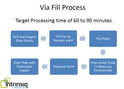
Now, for the exciting part, there are two distinct advantages for PCB manufacturing with this product. First, because it is run with commercially available equipment, as seen in the process flow diagram, the capital investment needed to offer copper-filled via technology is significantly reduced. Many printed circuit board manufacturers are not able to offer the copper-filled via option due to the cost of plating equipment and chemistries. The barrier to entry for these PCB manufactures will be eliminated.
The second exciting benefit to this technology is the process time requirement. Solid copper-plated vias typically require 4 to 6 hours of plating time by the manufacturer, along with the specialized equipment and chemistry. This new product will enable PCB manufacturers to produce copper-filled vias in 60-90 minutes. A shortened cycle time will have benefits in lead-time and processing costs.
Product release for this screen printable paste is currently scheduled for the end of 2016. Throughout this year, pilot programs will be released, further testing completed and reliability data gathered.
Product development, an interesting process
Nano copper inks and pastes are typically sintered photonically with broadband (xenon) flash or near IR laser. Because the copper cladding is too thermally conductive to allow complete sintering and high power lasers are a barrier to entry due to cost and complexity, an oven solution was sought to keep the process compatible with existing technology. Heller Industries manufacturers a formic acid environment convection oven to be used for flux-less reflow. This was determined to be the perfect environment to sinter nano copper without oxidation. Nano copper paste can be completely sintered in 40 minutes or less.
The process development for this product has had several iterations. The initial proof of concept was to deposit paste into mechanically drilled blind vias using a vacuum bag to help fill the holes. Those initial coupons were plated and etched prior to filling to allow for laser sintering. As the development progressed, the testing moved to copper clad PCB’s with mechanical blind vias. The panels were electroless copper plated then electroplated to simulate actual via filling requirements. Unfortunately, the thermal conductivity of the copper foil prevented the ability to sinter the copper paste. Research then pointed to thermal sintering in a formic acid environment.
As the development process continued, it was determined that the extended time necessary for formic acid sintering at 250C destroyed the PCB laminate. Moving forward, other nano additives were included in the formulation to lower the temperature requirement to 225C. This formulation and temperature sintered the vias completely in 60 minutes.
The next phase in the development process was to screen print trace patterns on FR-4 to be sintered alongside the via filled coupons. These samples were used to calculate bulk resistivity as compared to copper. Typical measurements were 6X to 8X that of bulk copper. Typical epoxy-based conductive via fills are in the 20X to 50X range.
Today’s product
Moving forward, additional product development was undertaken resulting in the current formulation, which allows the sintering temperature to be reduced to 190C. The paste is sintered to pure copper in only 40 minutes in the Heller conveyor oven. Samples of this formulation were via filled using the vacuum bag technique, on copper clad panels, with copper plated blind vias. The panels were Heller sintered, planarized, over-plated and solder floated. Samples were then subjected to IPC standard reliability testing parameters. Each sample was floated at 288C, held at temperature for 10 seconds, cooled, and refloated 4 times. The vias survived 5 solder float procedures.
It is always exciting to learn about the new developments in products and processes for the PCB industry. In this case, incorporating nano copper inks and pastes into standard printed circuit board manufacturing techniques will allow manufacturers to offer a solid copper-via option to their customers without significant capital investment in specialized plating equipment.
Please contact us for more information. http://www.omnipcb.com tarad@omnipcb.com
